

How the PCB Panel creat and seperate?
How the PCB Panel creat and seperate?
For cost-saving or technical reasons (such as improved assembly),multiple circuit boards may be combined to form a “panel”. This panel is then produced just as a single large circuit board. A separation of the panel does not occur!Always clarify the panel design with your assembly partner; pay attention to fiducials marks or mounting holes!
1.Panel types:
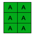
--Multiplier panel:Identical PCBs within panel
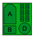
--Mixed multiplier panel:Different PCBs within panel
2.Mechanical processing
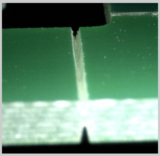
--Scoring
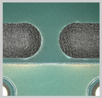
--Milling with bridges / with bridges and mousebites
--Milling / scoring combination
--without mech. processing
3.X-out
--Standard: A damaged printed circuit board (according to E-test) is not removed from the panel, but marked (X-out). This must be taken into account for assembly.
--Special production: If you do not want an X-out, Please mentioned it to the fabricator.
4.Mechanical processing / Panel separation
--Scored
--Milled with bridges
----Milled with bridges & mousebites
5.Design Parameters
6.Multiplier panel
Multiple identical circuit board layouts are composed to form one panel. The completed panel is scored, or partially milled-out to provided the contained PCBs with bridges for breaking out.
7.Multiplier scored
When designing the panel, please observe that a spacing of 0,0mm is left between the circuit boards. If a spacing between the (scored) PCBs is required, please leave a gap of min. 5,0mm.
The contour line thickness should be 0,01mm / 1 mil.
Because of the tolerances when breaking out the single circuit boards, all conductor traces and copper areas should have a spacing of at least 500µm from the scoring edge (see V-Scoring)
We recommend using scoring technology only for panels with a circuit board thickness of at least 1mm (stability).
Example:Simple panel scored
--The panel design should always be checked with your assembly partner,Pay attention to fiducial marks and mounting holes!
--Minimum space between tracks / copper and scoring edge:500um!
--Spacing between the single boards:0.0mm!
--Define outlines with 0.01mm or 1mil!
--We suggest a frame of 5-10mm for better handling!
8.Multiplier milled
When designing the panel, please observe that a spacing of 2,0mm is left between the circuit boards.
All conductor traces and copper areas should have a spacing of at least 200µm from the milling edge.
If no bridges are defined by the customer, these will be inserted by Multi CB! Optimum width for the bridges: 1,0 - 1,5mm.
Example:Simple panel scored
--The panel design should always be checked with your assembly partner,Pay attention to fiducial marks and mounting holes!
--Minimum space between tracks / copper and scoring edge:200um!
--Diemeter of milling-tool,always 2.0mm!
--If you place the bridges by yourself,use a width of 1-1.5mm!
--We recommend a frame of 5-10mm for better handling!
9.Mixed multiplier panels
For complex panels, multiple different circuit board layouts can be composed onto one panel. The completed panel is scored, or partially milled, to provided the contained PCBs with bridges for breaking out.
10.Mixed multiplier scored
When designing the panel, please observe that a spacing of 0,0mm is left between the circuit boards. If a spacing between the (scored) PCBs is required,
please leave a gap of min. 5,0mm. For jump scoring a distance of 15mm is required.
The contour line thickness should be 0.01mm / 1 mil.
Because of the tolerances when breaking out the individual circuit boards, all conductor traces and copper areas should have a spacing of at least 500µm from the scoring edge (see scoring).
We recommend using scoring technology only for panels with a circuit board thickness of at least 1,0mm (stability).
11.Mixed multiplier milled
When designing the panel, please observe that a spacing of 2,0mm is left between the circuit boards. For reasons of stability, a distance of 10mm is usually recommended.
All conductor traces and copper areas should have a spacing of at least 200µm from the milling edge.
If no bridges are defined by the customer, these will be inserted by Multi CB Optimum width for the bridges: 1,0 to 1,5mm.
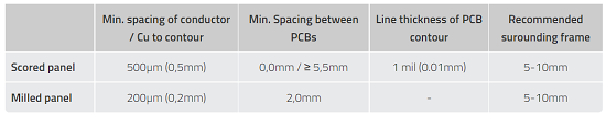
12.Example for milling/scoring combination
When designing the panel, please observe that a spacing of 0,0mm is calculated between scored parts, and preferably 2,0mm between milled parts.
All conductor traces and copper areas should have a spacing of at least 500µm from the scoring edge, and at least 200µm from the milling edge!
13.Milling/scoring combination hassle-free
If the outer edge of the milling lies on the scoring line, the milling tool moves along the scored base material. This increases the risk of forming of chips.
Advice: Do not mill directly aligned with scribe lines.
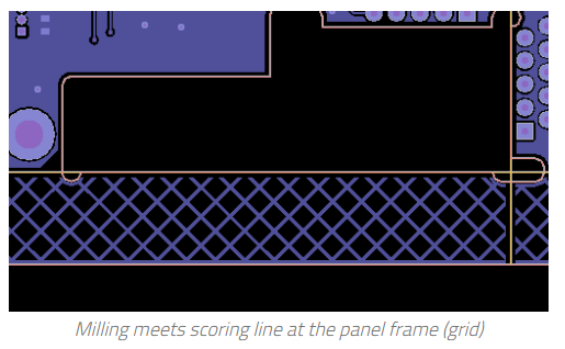
We manufacture PCBs with milling and scoring on the same line. Should this result in shaving (chip) formation, a reclamation in this regard would be rejected.
PCB Blog
Contact Us
E-mail: [email protected]
E-mail: [email protected]
Skype: [email protected]
Whatsapp: +86 15012972502
Add: 2F, BUILDING H, WANDA INDUSTRIAL ZONE, ZHOUSHI ROAD, LANGXIN COMMUNITY,SHIYAN STREET, BAO 'AN DISTRICT, SHENZHEN, GUANGDONG, CHINA


 Skype Chat
 WhatsApp
  Mail inquiry