

What causes PCB bow and twist?-Moisture
What causes PCB bow and twist?-Moisture
The PCB fabrication process requires multiple trips through various chemical baths, rinses and washes. It's easy for liquid or gasses to become trapped within the fiberglass weave or inside plugged or tented vias. One of the final steps in the PCB fabrication process is to bake the boards at a low temperature (248°F – 266°F / 120°C – 130°C) for several hours while inside a press. It is still possible for moisture or gasses to remain trapped inside the board even after this process, but it should be minimal at this stage.
It's also possible for moisture to wick into the board simply by absorbing the ambient humidity in the air. If you are storing boards on a shelf for any amount of time, it's advised to reseal any open board packs with a desiccant, not only to prevent unwanted moisture but also to slow the degradation of the surface finish.
TIP: At PCB Prime, we will package your boards in an airtight shrink wrap along with a desiccant to prevent moisture absorption during transit or storage.
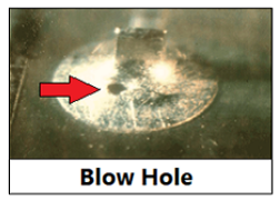
During assembly, any trapped liquids or gasses will try to escape when the board is heated to reflow temperatures. This evacuation is called outgassing. In extreme cases, outgassing can cause components to be physically ejected from the board during the assembly process. Outgassing may also cause other damage such as measling, delamination, blow holes, and sunken solder fillets.
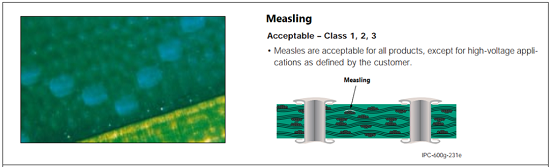
(From IPC-A-600G)
Measling manifests itself in the form of discrete white squares or "crosses: below the surface of the base material, and is usually related to thermally induced stress. Measles are subsurface phenomena that have been found in new laminated materials and in every board type made from woven fiber reinforced laminates at one time or another. Since measles are strictly subsurface phenomena and occur as a separation of fiber bundles at fiber intersections, their apparent positions relative to surface conductors have no significance.
Delamination is a separation between plies within a base material, between a material and conductive foil, or any other planar separations within a printed board.
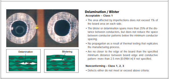
Blister is a delamination in the form of a localized swelling and separation between any of the layers of a lamination base material, or between the base material and conductive foil or protective coating.
Blow holes are demonstrated by small voids in through hole solder joints. If the copper plating in the barrel of the holes is thin, weakened, or cracked, it can allow gasses to escape during assembly.
Sunken Solder Fillets can be caused by outgassing caused by trapped moisture or gasses escaping the laminate during assembly. If the copper plating lining the hole wall is at or above the IPC standard 25µm, then the copper should prevent outgassing. Other causes for sunken solder fillets are:
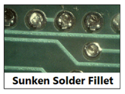
--Incorrect hole to lead size ratio, where the component lead is not large enough to support the weight of the solder. There won't be enough solder to fill the hole above the surface of the laminate.
--Contamination or foreign inclusion in the hole preventing proper solder flow.
--Improper heating or insufficient flux.
What causes PCB bow and twist?-Uneven Copper Distribution
What causes PCB bow and twist?-Unbalanced Stack Up
What causes PCB bow and twist?-Pre-Preg Materials Arranged Incorrectly
What causes PCB bow and twist?-Mixed Material Types
What causes PCB bow and twist?-Finished Thickness
What causes PCB bow and twist?-Moisture
What causes PCB bow and twist?-Rapid Heating During Assembly
What causes PCB bow and twist?-Assembly Conveyor Setup
PCB Blog
Contact Us
E-mail: [email protected]
E-mail: [email protected]
Skype: [email protected]
Whatsapp: +86 15012972502
Add: 2F, BUILDING H, WANDA INDUSTRIAL ZONE, ZHOUSHI ROAD, LANGXIN COMMUNITY,SHIYAN STREET, BAO 'AN DISTRICT, SHENZHEN, GUANGDONG, CHINA


 Skype Chat
 WhatsApp
  Mail inquiry