PCB fab drawing example
In the world of printed circuit board (PCB) manufacturing, a clear and accurate PCB fabrication drawing (fab drawing) is the cornerstone of successful production. It serves as the critical bridge between design concepts and physical PCB realization, ensuring that every detail—from trace widths to component placement—aligns with the designer’s intent. For manufacturers specializing in high-performance PCBs like RF PCB, HDI PCB, large-size PCB, and special PCB, a well-crafted fab drawing is even more essential to maintain precision and performance. At Hopetime PCB, we leverage decades of experience in RF PCB fabrication, large-size PCB production, large-size PCB assembly (SMT), HDI PCB manufacturing, and special PCB production to create industry-leading fab drawings. In this guide, we’ll walk you through a detailed PCB fab drawing example, highlight key elements, and explain how our expertise elevates fab drawing quality for specialized PCB types.
What is a PCB Fab Drawing?
A PCB fab drawing (also known as a fabrication print) is a detailed technical document that provides all necessary specifications and instructions for PCB manufacturers to produce a board accurately. Unlike design files (such as Gerber or ODB++), fab drawings consolidate critical information in a single, easy-to-reference format—making it easier for CAM operators, engineers, and production teams to verify details and avoid errors. This document is particularly vital for complex PCBs, including RF PCB (high-frequency PCB), HDI PCB (high-density interconnect PCB), large-size PCB, and special PCB, where even minor deviations can compromise performance, fit, or functionality.
At Hopetime PCB, our fab drawings are tailored to the unique requirements of each PCB type, ensuring that the specific needs of RF signal integrity, HDI density, large-size stability, and special material compatibility are clearly communicated. Below is a step-by-step PCB fab drawing example, with a focus on how we address the nuances of our core advantage products (core products).
PCB Fab Drawing Example: Key Elements & Specifications
To illustrate a practical fab drawing, we’ll use a multi-layer RF PCB example—one of our most in-demand products—with additional notes for HDI PCB, large-size PCB, and special PCB. This example aligns with IPC standards (IPC-6012, IPC-A-600) and incorporates the critical details that set Hopetime PCB apart in RF PCB fabrication and beyond.
1. Title Block & Basic Information
The title block is the first section of any fab drawing, providing essential administrative and project details. For our RF PCB example, the title block includes:
- Project Name/Number: RF-2026-001 (High-Frequency PCB for 5G Communication)
- PCB Type: RF PCB (High-Frequency, 6-Layer)
- Dimensions: 180mm x 120mm (Standard RF PCB Size; for large-size PCB, dimensions would be ≥500mm x 500mm, with special notes on warpage control)
- Fabricator: Hopetime PCB (www.hopetimepcb.com) – Specializing in RF PCB, HDI PCB, Large-Size PCB Production, Large-Size PCB assembly, Special PCB manufacturing.
- Revision Number: Rev. A (with revision date and change notes)
- Designer/Approval Signatures: To ensure accountability
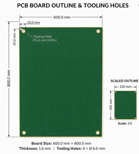
2. Board Outline & Dimensions
The board outline is a precise drawing of the PCB’s shape, with all critical dimensions labeled. For our RF PCB example:
- Outline Dimensions: 180mm (length) x 120mm (width) x 1.6mm (thickness)
- Tolerances: ±0.1mm (critical for RF PCB to ensure fit with enclosures and signal integrity; for large-size PCB, tolerances are tightened to ±0.2mm to prevent warpage)
- Tooling Holes: 4 x 3mm non-plated holes (NPTH) at each corner, positioned 10mm from the edge (for large-size PCB, additional tooling holes are added to support handling during fabrication and PCB assembly)
- Cutouts/Notches: 15mm x 10mm notch on the top edge (for connector access, common in RF communication devices)
3.Layer Stackup (Critical for RF & HDI PCB)
The layer stackup section is vital for RF PCB and HDI PCB, as it directly impacts impedance control, signal crosstalk, and thermal performance. Our RF PCB example stackup (4-layer) includes:
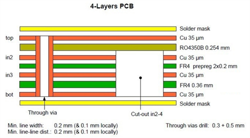 *RF Mix laminate PCB sturcture - Stack up
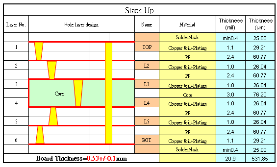 *HDI PCB structure - Stack up
Notes for Specialized PCBs:
- HDI PCB: A 10-layer HDI PCB fab drawing would include microvias (60μm diameter), blind/buried vias, and a 2+N+2 stackup (outer layers with two-order microvias) – critical for high-density packaging in consumer electronics. Hopetime PCB’s HDI PCB fabrication supports line widths/spacings down to 50μm/50μm.
- Large-Size PCB: Such as a 600mm x 800mm large-size PCB, the stackup includes thicker core materials (e.g., 1.6mm FR-4) and reinforced copper layers (2oz) to prevent warpage during fabrication and PCB assembly. Our large-size PCB production process includes specialized pressing and curing to maintain flatness.
- Special PCB: For special PCB (e.g., high-temperature PCB, rigid-flex PCB), the stackup specifies unique materials (e.g., polyimide for high-temperature resistance) and layer configurations tailored to the application (e.g., flexible sections for rigid-flex PCB)
4.Drill Chart & Drill Map (Essential for All PCB Types)
The drill chart and drill map specify all holes (plated and non-plated) in the PCB, a critical detail for fabrication accuracy. Our RF PCB example includes:
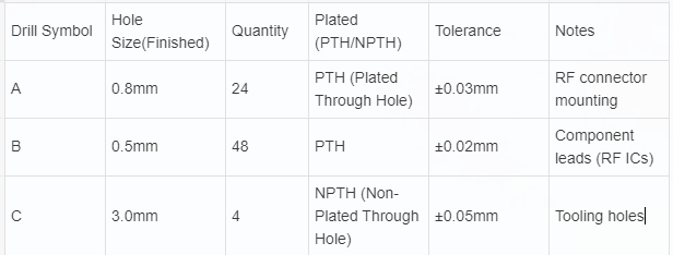
The drill map is a visual representation of all holes, with each hole marked with its corresponding drill symbol. For HDI PCB, the drill map includes microvia positions and symbols; for large-size PCB, the drill map is scaled to show hole distribution across the entire board, with notes on drilling sequence to prevent board warpage. For special PCB (e.g., blind via PCB), the drill map distinguishes between blind, buried, and through holes.
5. Surface Finish & Solder Mask Specifications
Surface finish and solder mask directly impact PCB durability, solderability, and performance—especially for RF PCB and HDI PCB. Our RF PCB example specifies:
- Surface Finish: ENIG (Electroless Nickel Immersion Gold) – 2.5μm nickel, 0.05μm gold. Ideal for RF PCB as it provides excellent signal integrity, corrosion resistance, and compatibility with SMT components. For large-size PCB SMT, ENIG ensures uniform solderability across the entire board.
- Solder Mask: Green (ROHS-Compliant), with 0.1mm clearance around all pads and traces. For RF PCB, solder mask is applied with precision to avoid covering RF traces (critical for impedance control). For HDI PCB, solder mask is thinned to accommodate fine-pitch components.
- Silkscreen: White silkscreen, with 0.15mm line width for component labels (e.g., “U1” for RF IC, “C1” for capacitors). For large-size PCB, silkscreen is scaled to ensure readability across the board.
Notes for Special PCB: For high-temperature special PCB, we specify a high-temperature solder mask (e.g., polyimide-based) that can withstand operating temperatures up to 260°C. For rigid-flex special PCB, solder mask is applied only to rigid sections to maintain flexibility.
6. Special Instructions & Tolerances
This section addresses unique requirements for specialized PCBs, ensuring that manufacturers understand critical process steps. For our RF PCB example, special instructions include:
- Impedance Control: 50Ω for all RF traces (±5% tolerance) – critical for 5G signal integrity. Hopetime PCB’s RF PCB fabrication uses advanced impedance simulation to ensure compliance.
- RF Trace Requirements: No sharp corners (minimum 0.5mm radius) to prevent signal reflection; trace width maintained at 1.2mm for 50Ω impedance.
- Testing Requirements: 100% electrical testing (E-test) to verify continuity and isolation; RF performance testing (S-parameters) to ensure signal integrity.
- For Large-Size PCB: Warpage control ≤0.5mm/m; specialized handling during SMT to prevent bending (Hopetime PCB’s large-size PCB SMT uses custom fixtures for stability).
- For HDI PCB: Microvia inspection using 5D AOI (Automated Optical Inspection) to ensure drill accuracy; resin filling for microvias to prevent solder bridging.
- For Special PCB: Material certification (e.g., RoHS, REACH) for all components; thermal testing for high-temperature special PCB.



 Skype Chat
 WhatsApp
 Mail inquiry