What are Warp & Twist in PCB?
What are Warp & Twist in PCB?
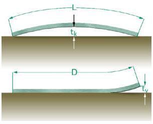
Warp & Twist are the two characteristics used to determine the flatness of printed circuit boards.

Warp determination :
The percentage K of the deflection (tk) relative to the length (L) of the curved edge
K= tk/L*100 %
If the warp occurs both lengthwise and crosswise, the largest value counts.
Twist determination :
Twist is the percentage V of the deflection (tv) relative to the length (D) of the diagonal:
V=tv/D *100 %
PCB Bow and Twist
Bow and twist are the two characteristics used to determine the flatness of printed circuit boards. The bow condition is a spherical or cylindrical curvature of the board, when its four corners lie in the same plane. However, twist is the condition where the deformation lies parallel to the diagonal of the circuit board. This means one corner is different than the other three corners. As per the IPC-A-600 standard, all boards should have bow and twist less than 1.5%. For boards with SMD components, the bow and twist values should be less than 0.75% or less. At Twisted Traces, we provide printed circuit boards with SMT values ≤0.75%, and non-SMT values ≤1%.
Steps Taken To Avoid Bow And Twist
Bow and twist is affected by the board designs. Material properties and board thickness are the two other factors influencing the board design. At Twisted Traces, PCB designing and assembly is handled by qualified and expert PCB designers. They take the following steps to avoid bows and twists:
1.A symmetrical build-up of copper thicknesses, pre-pegs, and cores is selected in the PCB manufacturing process. The risk of bows and twists is high in multilayered circuit boards. This risk is minimized by adding pre-peg to the mix.
4.Copper distribution is the key factor that we concentrate upon. Unbalanced copper weights have negative impact on bow and twist. If there are areas with low or high density copper distribution, our designers add copper to balance the low density areas.
Go to the PCB knowledge Page
Go to the PCB design resources page
Back to the technology data
PCB Blog
Contact Us
E-mail: [email protected]
E-mail: [email protected]
Skype: [email protected]
Whatsapp: +86 15012972502
Add: 2F, BUILDING H, WANDA INDUSTRIAL ZONE, ZHOUSHI ROAD, LANGXIN COMMUNITY,SHIYAN STREET, BAO 'AN DISTRICT, SHENZHEN, GUANGDONG, CHINA


 Skype Chat
 WhatsApp
  Mail inquiry