

Products >> COB Bonding Manufacturing
What is COB Bonding Manufacturing?
Short for Chip On Board, COB is a system where semiconductor dice are mounted directly on a PCB board and connected with either bonded wires or solder bumps.
Advantages offered by COB technology include: 1) reduced space requirements; 2) reduced cost; 3) better performance due to decreased interconnection lengths and resistances; 4) higher reliability due to better heat distribution and a lower number of solder joints; 5) shorter time-to-market; and 6) better protection against reverse-engineering.
The general term for COB technology is actually 'direct chip attachment', or DCA. Aside from circuit boards used for COB's, various substrates are available for use in DCA. There are, for instance, ceramic and glass ceramic substrates which exhibit excellent dielectric and thermal properties. Organic substrates that weigh and cost less while providing a low dielectric constant also exist. There are also flex substrates which, being pliable, have the ability to bend. DCA assemblies have received a number of other names aside from 'COB' based on these available substrates, e.g., chip-on-glass (COG), chip-on-flex (COF), etc.
The COB process consists of just three major steps: 1) die attach or die mount; 2) wirebonding; and 3) encapsulation of the die and wires. A variant of COB assembly, the flip-chip on board (FCOB), does not require wirebonding since it employs a chip whose bond pads are bumped, which are the ones that connect directly to designated pads on the board. As such, FCOB's have their chips facing downward on the board (hence the name 'flipchip'). Aside from encapsulation, it is also necessary to 'underfill' a flip chip to protect its active surface and bumps from thermo-mechanical and chemical damage. 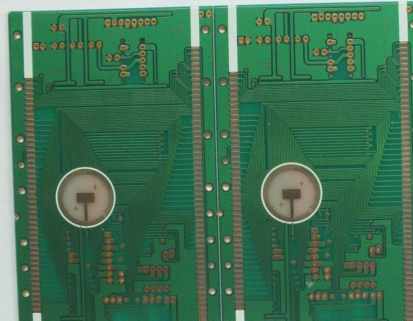
Figure 1. Example of a Chip-on-Board (COB) Assembly; note that the chips are directly wirebonded to the PCB
Die attach basically consists of applying a die attach adhesive to the board or substrate and mounting the chip or die over this die attach material. Adhesive application may be in the form of dispensing, stencil printing, or pin transfer. Die placement must be accurate enough to ensure proper orientation and good planarity of the die. This is followed by a curing process (such as exposure to heat or ultraviolet light) that allows the adhesive to attain its final mechanical, thermal, and electrical properties. After curing, organic contaminants must be removed either by plasma or solvent cleaning so as not to affect the wirebonding process.
The wirebonding process is similar to that used in traditional semiconductor assembly, i.e., thermosonic Au or Cu ball bonding or ultrasonic Al wedge bonding may be employed to connect wires between the die and the board or substrate. Chip-to-chip wirebonding may also be done for COB assembly. Needless to say, the bond pads of the die and the board or substrate must be free of any contaminants and defects to ensure the formation of good and reliable bonds.
Finally, the die and bond wires are encapsulated to protect them from mechanical and chemical damage. Encapsulation is generally done by dispensing a liquid encapsulant material (usually epoxy-based) over the die and wires or by transfer molding. Encapsulants also need to undergo curing, the process of which depends on the type of encapsulant used.
Products Category
- PCB Design & Layout
- PCB manufacturing
- PCB Assembly
- BGA Assembly
- THT Assembly
- SMT Assembly
- Mixed PCB Assembly in Electronic PCBA
- Single sided PCB assembly
- Double sided PCB assembly
- Rigid-Flex Assembly
- COB Bonding Manufacturing
- Components sourcing for PCB Assembly
- SMT Stencils
- Box build assembly
- PCB engineer reverse
Contact Us
E-mail: [email protected]
E-mail: [email protected]
Skype: [email protected]
Whatsapp: +86 15012972502
Add: 2F, BUILDING H, WANDA INDUSTRIAL ZONE, ZHOUSHI ROAD, LANGXIN COMMUNITY,SHIYAN STREET, BAO 'AN DISTRICT, SHENZHEN, GUANGDONG, CHINA


 Skype Chat
 WhatsApp
  Mail inquiry