PCB Design Guidelines
PCB Design Guidelines
Below are are general rules that apply for the most PCB fabricators, but it is advisable to check with your fabricator.
Trace Width and Spacing
The chemical and photographic processes used to produce a PCB put requirements on the minimum width of trace and the minimum spacing between traces. If a trace is made smaller than this minimum width there is some chance it will open (no connection) when manufactured. If two traces are closer together than the minimum spacing there is some chance they will short when manufactured. These parameters are usually specified as "x/y rules", where x is the minimum trace width and y is the minimum trace spacing. For example, "8/10 rules" would indicate 8 mil minimum trace width and 10 mil minimum trace spacing. These rules (especially spacing) apply to any metal on the PCB, including pad to track spacing and line widths for strings on the PCB.
Typical modern process rules are 8/8 rules with values as small as 2/2 rules being available. For Press-n-Peel people have had success using 12/12 rules, but values a little larger are easier to make work consistently. However, keep in mind that the board must be soldered and a trace within 8 mils (8/8 rules) of a pad is easier to short than one with greater spacing when hand soldered. For hand soldering 10/10 rules are much easier to solder (if the design density can allow spacing this large).
Board Size
PCB manufacturers have a maximum size board they can handle. Typically this is also their panel size. The PCB fabrication house's panel size is also important when mass producing boards. In this situation one would want to fit as many boards as possible on a panel with as little wasted board space as possible (in order to reduce costs). Normal board spacing for routing (how boards are separated on a panel) is 0.3", plus there is typically a 1.0" to 2.0" border on the board for handling it during processing.
Board thickness may also be specified. A standard thickness and type of board is .062" FR4. Other typical board thickness are .010", .020", .031", and .092".
Pad Sizes
The biggest issues with pad size are solder ability and manufacturability. Solder ability is really just a matter of skill and will not be discussed here. Manufacturability is concerned with whether or not the pad will be broken when the hold is drilled in it. This is mainly a function of the accuracy of the PCB manufacturer's drilling. If a drill hole is slightly off center the pad may be broken at one edge possibly leading to an open in the circuit. A standard requirement for pad sizes is a 5 mil annulus. This means there must be .005" all around the hole (i.e. a 28 mil hole would require a 38 mil pad). Something a little larger than this (maybe 10 mils) is recommended for solder ability. AP Circuits states they have had relatively consistent success with a 2.5 mil annulus (i.e. a 20 mil hole with only a 25 mil pad), but they don't recommend it.
Hole Sizes
Most PCB manufacturers have a wide selection of drill (hole) sizes available. Some charge per drill size used, others offer a standard set of drill sizes for no charge and then charge for any non-standard drill sizes. AP Circuits uses the latter approach. When choosing a hole size remember that the plate-through will cause the hole to effectively be more narrow. The plate-through thickness varies from .001" to .003". AP Circuits' plate-through thickness is approximately .015" (meaning the "finished hole" diameter is 3 mils smaller).

Hole Density
Hole density is purely a cost issue. The more holes there are on a board the more wear and tear manufacturing will put on the equipment (and thus the more the board will cost). Most PCB manufacturers have a maximum hole density and boards with greater density are charged more. For AP Circuits, there is a per hole charge for densities above 24 holes per square inch.

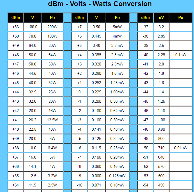
Getek® Laminates - Epoxy / Polyphenylene Oxide Resin
(Type: NEMA FR-4, IPC-L-108B/04)
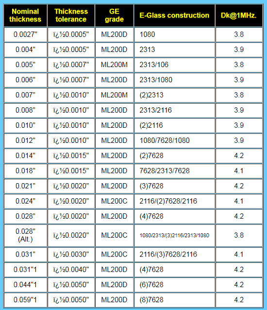
VSWR Vs. Return Loss

VSWR Vs. Return Loss (Continued)
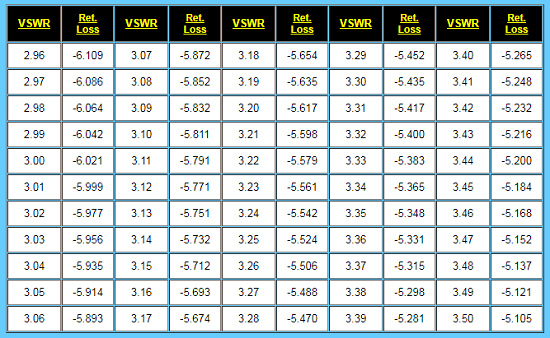
WIRE DATA CHART

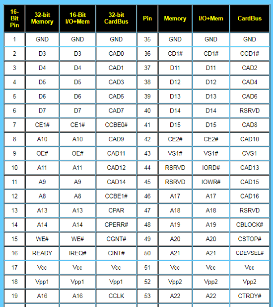
PCMCIA CONNECTOR PIN OUT
TRACE SPACING GUIDELINE
Voltage Between Conductors
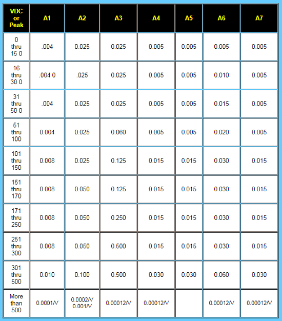
A1 - Internal Conductors
A2 - External Conductors, uncoated, sea level to 10,000 ft.
A3 - External Conductors, uncoated, over 10,000 ft.
A4 - External Conductors, with permanent polymer coating (Solder Mask).
A5 - External Conductors, with conformal coating over assembly.
A6 - External Component lead/termination, uncoated.
A7 - External Component lead/termination, with conformal coating.
Electrical Design Factors
Conductor Capacitance
C = 0.31 a/b + 0.23(1 + k) log10 (1 + 2b/d +2b + b2/d2)
Where
k = Substrate dielectric constant
a = Conductor thickness
b = Width of conductor in inches
d = Distance between conductors in inches
Conductor Resistance
R = 0.000227W
Where
W = Width of conductor
Characteristic Impedance
Zo = R + jwL / G + kwC
Where
Zo = Apparent Z of an infinitely long line in ohms
R = Resistance in ohms
L = Inductance in Henries
G = Conductor per unit length of line in mhos
C = Capacitance in farads
Characteristic Impedance for a Micro Strip
Zo = (h/W) (377 / (Sqrt. er) {1 + (2h/PI W)[1 + ln(PI W/h)]}
Where
h = Dielectric thickness
W = Micro Strip width
er = Effective dielectric constant of substrate
Go to the PCB knowledge Page
Go to the PCB design resources page
Back to the technology data
PCB Blog
Contact Us
E-mail: [email protected]
E-mail: [email protected]
Skype: [email protected]
Whatsapp: +86 15012972502
Add: 2F, BUILDING H, WANDA INDUSTRIAL ZONE, ZHOUSHI ROAD, LANGXIN COMMUNITY,SHIYAN STREET, BAO 'AN DISTRICT, SHENZHEN, GUANGDONG, CHINA



 Skype Chat
 WhatsApp
  Mail inquiry