

Copper Layers
PCB Design Guidelines-Copper Layers
We refer to Copper Layers as a layer of a PCB that has copper on it after etching, usually tracks and pads or power and ground layers.
Generating Output Files for Copper Layers
When generating output data files use “flashes” for pads and avoid “painted/drawn” pads.
For larger copper areas or copper planes avoid filling them with small draws (“painting”).
Where possible, use contours or polygons to construct areas or planes, these are standard features in Gerber X2 output as well as other data formats.
Always include the board outline when you output your copper layers as this helps us to identify any data alignment, rotation or mirroring issues.
This is best done using a small line – e.g. 0.50mm (20mil) wide – where the centre of the line is the exact board outline.
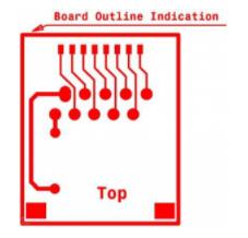
We will remove this line from the production data we produce for the manufacturing process.
Non-Plated Through Holes (NPTH)
Remove copper pads from NPTH holes if these pads are not used or connected to other copper before generating the output data files.
If you require copper pads on NPTH holes please use a minimum Outer Annular Ring (OAR) of 0.30mm (12mil) as defined in our PCB Design Guidelines – Classification page.
Copper Webs and Slivers
Check your final design for small areas of unconnected copper or narrow copper webs and slivers which can lead to problems in production.
Copper to Board Edge Clearance
The minimal clearance between edge of board and pattern is.
For routed boards:
*0.25mm (10mil) on outer layers
*0.40mm (16mil) on inner layers
For boards with scoring (V-cut):
*0.45mm (18mil) on outer and inner layers
If you require a copper area or plane to extend up to the board edge please clearly indicate this in the Mechanical Layer.Copper up to the board edge should only be used where absolutely necessary due to:
*There is a risk of a rough board edge as the copper may tear during contour routing (profiling).
*The copper can create electrical shorts between layers.
*Copper up to the board edge is NOT compatible with scoring (V-cut).
Board Edge Plating
If you require the board edge or part of it to be plated, then clearly indicate this in the Mechanical Layer.
In addition, were the board edge is to be plate there must be copper placed on the top and bottom layers with a minimum width of 0.5mm from the edge of the board inwards.
This is necessary to enable us to produce the Round Edge Plating in such a way, that the metallisation is physically strong enough to stay attached to the side of the board.
Text Placed on Copper Layers
Any text placed in a copper layer has to comply with the design rules for the given class as defined in our PCB Design Guidelines – Classification page.
All copper text must be correctly readable after etching.A PCB is always viewed from top to bottom through the PCB.Therefore, the text on the top layer of your board should be readable and the text on the bottom layer should be non-readable or mirrored.
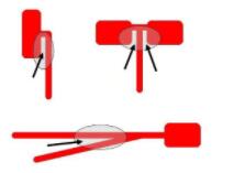
Avoid “Peelables”
“Peelables” occur during production and are small/narrow pieces of photo resist enclosed by pads, traces and/or planes.
These may “peel” away during processing and cause short or open circuits.All copper even within the same net must comply with the design rules for the given class as defined in our PCB Design Guidelines – Classification page.
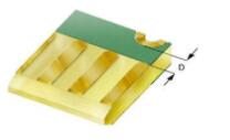
Gold Edge Connectors
For gold connectors do not place any plated holes (PTH), SMD or other pads closer than 2.00mm (80mil) to the gold fingers – see the drawing below.
Layer Sequence
ALWAYS provide the proper layer sequence for a multilayer board.
The layer sequence can be given in several ways:
*Indicate the layer numbers in the copper image by placing a logical number in each layer (1 for top layer, 2 for inner1, 3 for inner2, etc….).
*Make sure the numbers are positioned in such a way that they do not overlap, and can be seen through the complete PCB.
.jpg)
*Name each layer file in a way which indicates clearly the sequence to be used (e.g. T(op), I(nner)1, I(nner)2, B(ottom).
*Include in your Mechanical Layer file a clear build-up drawing with the correct sequence and corresponding data file name including:
*All Copper Layers, Soldermask Layers and Legend Layers.
*Additional layers like peel-off or carbon.
*Include a simple ASCII text file with your data indicating which file is to be used for which layer, preferably already in the correct build-up sequence (this is the least preferred solution).
Recommendations
Holes not Connected to Inner Layers
It is recommended to REMOVE pads from inner layers that the hole does not connect too.
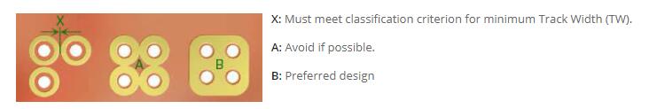
Thermal Pads
Ensure that the thermal relief pads are properly defined and comply with the chosen pattern classification for Annular Rings (AR), Track Widths (Thermal Segment Width) and Gaps.
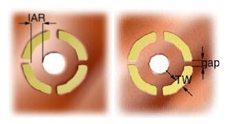
A good practice for Thermals is to work with a Gap of 0.20mm (8mil) and a Thermal Segment Width of 0.20mm (8mil).
Hatching Patterns
Use full copper rather than hatching patterns in copper planes.
If you need a hatching pattern, then use following minimum settings:
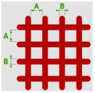
*Minimum distance or clearance between tracks of pattern (A): 0.40mm (16mil)
*Minimum track width for pattern (B): 0.20mm (8mil)
IMPORTANT
Any hatching pattern that DOES NOT meet these minimum requirements will be converted into a full copper plane.
Go to the PCB knowledge Page
Go to the PCB design resources page
Back to the technology data
PCB Blog
Contact Us
E-mail: [email protected]
E-mail: [email protected]
Skype: [email protected]
Whatsapp: +86 15012972502
Add: 2F, BUILDING H, WANDA INDUSTRIAL ZONE, ZHOUSHI ROAD, LANGXIN COMMUNITY,SHIYAN STREET, BAO 'AN DISTRICT, SHENZHEN, GUANGDONG, CHINA


 Skype Chat
 WhatsApp
  Mail inquiry