

What’s the reason for Solder balls or solder balling on PCB?
What’s the reason for Solder balls or solder balling on PCB?

Figure 1:Manual removal of this solder attachment will damage the track.
The solder has wet the track due to failure of the resist coating. The coating may have failed as it was applied over a tin/lead coating on the tracking or due to poor print thickness control.
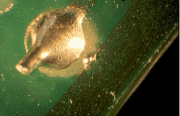
Figure 2: This solder ball must have attached itself to the resist as it separated from the pin.
Solder balling can be caused by poor process conditions with gassing from the flux during wave contact or excessive turbulence as the solder flows back into the bath which causes spitting.
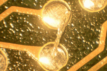
Figure 3: Another solder ball attached to the edge of a resist.
In Figure 3, a solder ball is attached to the base of the board on the edge of the resist and must have attached itself to the resist as it separated from the pin.
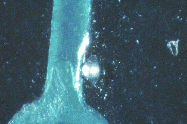
Figure 4: Solder on a resist can wet during wave contact and leave a ball.
Care should be taken with some solder balls. The example in Figure 4 is on a track and cannot be just knocked off. It is caused by squeeze out of the tin/lead from under the solder mask. or just simple adhesion.
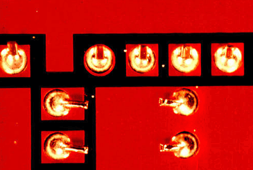
Figure 5: Solder balls on this board were caused by spitting from the surface of the wave
In Figure 5, the position of the balls is random. This type of defect is normally caused by spitting from the surface of the wave, which is associated with wave soldering parameters.

Figure 6: More solder balls caused by spitting.
Solder balls are caused by gassing and spitting of the flux on the surface of the wave or by solder literally bouncing back from the solder wave. This is caused by excessive back flow in air or too high
a drop in nitrogen environments.
Figure 7: More solder balling caused by spitting. Place a white card over the wave to pinpoint the cause of the problem.
The solder balling is random and more likely the result of solder balls spitting or bouncing up from the solder wave. This is caused by volatile materials still remaining from the flux or the height of the
wave separation.
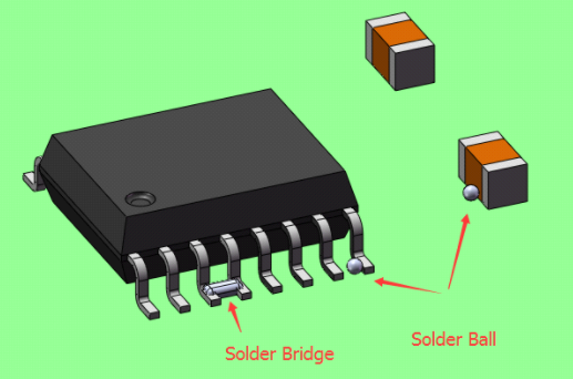
Figure 8:Solder Ball and Solder Bridge
A solder ball is the most common type of defect that occurs in the SMT assembly process. Solder balls, which have a diameter are greater than 0.13mm or they are within 0.13mm of traces, violate
the minimum electrical clearance principle. They can adversely affect the electrical reliability of the assembled PCB.According to the IPC A 610 standard, a PCB is also considered defective when there
are 5 solder balls (<=0.13mm) within 600mm^2.Analysis of Root Causes The solder ball is very closely related to air or water (trapped in solder paste) vapour escaping from the paste and turning into liquid. If the vapor in solder paste escapes too fast, a small amount of liquid
solder will be taken from from soldering joint, and a solder ball will be formed when it cools down. 1.PCB contains water. *Stored in an unexpectedly humid environment and isn’t dried before assembly. *PCB is too new and was not dried enough. 2.Too much flux is applied in the solder paste. 3.The preheat temperature is not high enough, so the flux has failed to effectively vapour out; 4.A solder paste printing issue due to the stencil not being clean, which causes the solder paste to stick to unexpected areas. Corrective Actions 1.Design the correct pad sizes and spaces according to the recommendation specified in the datasheet. 2.Reflow profile – when appropriate increase the preheating temperature. 3.Bake the PCB before printing. 4.PCB quality -- The thickness of PCB hole’s plating copper is greater than 25um in order to avoid trapping water in the PCB.
PCB Blog
Contact Us
E-mail: [email protected]
E-mail: [email protected]
Skype: [email protected]
Whatsapp: +86 15012972502
Add: 2F, BUILDING H, WANDA INDUSTRIAL ZONE, ZHOUSHI ROAD, LANGXIN COMMUNITY,SHIYAN STREET, BAO 'AN DISTRICT, SHENZHEN, GUANGDONG, CHINA


 Skype Chat
 WhatsApp
  Mail inquiry