

Outgassing on a pcba PCB after wave soldering
Outgassing on a pcba PCB after wave soldering
Outgassing is still a common problem associated with wave and hand soldering.
Most Common Reasons or Solutions:
*Poor pre heat process when using VOC free fluxes leads to spitting of very fine solder balls.
*This plating of less that 20um in the through hole or where the surface of the hole is so poor the plating does not cover broken glass bundles leading to gassing.
*In the old days you could have outgassing from the plating on pins but not to the degree shown.
Basically when a board is soldered any moisture in the board close to the hole is heated and turned to vapor. If there is thin plating or voids in the plating, gassing can come through the plated hole wall. If solder is present in the hole, this will produce voids in the solder as it solidifies. The voids may appear as small holes in the surface of the joint, as shown in Figure 1, or much larger cavities.
Having the correct copper plating thickness in the through holes is the key. A minimum of 25µm of copper should be present on the surface of the hole walls.
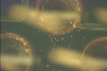
Figure 1: Voids caused by outgassing.
PCB Blog
Contact Us
E-mail: [email protected]
E-mail: [email protected]
Skype: [email protected]
Whatsapp: +86 15012972502
Add: 2F, BUILDING H, WANDA INDUSTRIAL ZONE, ZHOUSHI ROAD, LANGXIN COMMUNITY,SHIYAN STREET, BAO 'AN DISTRICT, SHENZHEN, GUANGDONG, CHINA


 Skype Chat
 WhatsApp
  Mail inquiry