

Design & Manufacturing Considerations for RF PCB Circuits
Design & Manufacturing Considerations for RF PCB Circuits
There are several key factors that engineers must consider when approaching an RF PCB manufacturing project.
1. Some constants, such as the dielectric constant, can be treated as a single value in non-RF applications, but they become more dynamic at the powerful frequency ranges of RF.
2. Managing heat within the board to ensure it survives the considerable thermal stresses of PCB assembly is vital. At the drill stage, the thermal properties of the material will play a critical role in layer-to-layer alignment of multilayer stacks.
3. The spacing of the features will play an important role as well, since RF PCB boards are prone to interacting with adjacent features in unexpected ways.
4. Choosing the proper materials based on the target application and budget is critical, since most of the remaining challenges will stem as a consequence of this choice.
Important Properties of RF PCB Materials
Choosing the right material is arguably the most critical decision in the RF PCB board manufacturing process.Many of the other key factors that affect the board’s performance, manufacturability and cost start here. Before considering material selection, it’s important to understand the key properties that define RF PCB board materials.
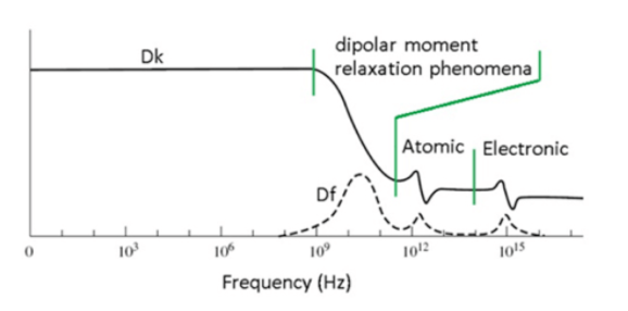
Plot of a Dk / Df vs. Frequency curve for a generic material. Using a generic material, this plot shows the change in dielectric constant for a PCB material from its lowest frequencies to its highest frequencies, with the effects of the material’s dipole moments.
The Dynamic Dielectric Constant
The dielectric constant measures a material’s ability to store electrical energy in an electric field.
It is direction-dependent, so the dielectric constant can change depending on the axis of the material. Unfortunately, it can shift under the high frequency conditions of RF, so it can’t be taken at face-value.
It’s important to understand what frequency range the material was tested under, what testing method was used and if there are values available for frequency ranges and conditions that closely match your target application.
The Coefficient of Thermal Expansion
The coefficient of thermal expansion (CTE) explains how an object’s size varies with a change in temperature. It is also a way to measure thermal robustness. It has a huge impact on the drill and assembly stages of PCB manufacturing.
In a multilayer stack, different materials with different CTE’s are going to change shape at different rates. When the layer above grows faster than the layer below, alignment becomes a serious problem during the drilling process.PTFE, one of the most commonly used RF materials due to its high quality, can smear at drill if it gets too hot and that can’t be removed. At the assembly stage, when components are being soldered on, the CTE affects how well it will handle the thermal stress of soldering. A poor CTE can lead to a broken board during its final stage of production, which is an expensive mistake best avoided.To mitigate these problems, a material with a lower CTE is going to handle the physical punishment of drill and assembly better.
Loss Tangent
Loss Tangent, like the dynamic dielectric constant, is one of those challenging effects that manifests in RF but isn’t as problematic for lower frequency designs. It’s a consequence of the molecular structure of the material itself.
As the frequency goes up, the signal loss occurs because it gets burned off as heat. In an analog circuit, amplitude loss occurs..In complex multilayer boards, components can become quite dense and additional heat generated during operation is something that needs to be considered.
Spacing
Spacing can be tricky in RF applications, due to crosstalk and something referred to as the “skin effect.”
Crosstalk is when the board begins interacting with itself, such as signals bleeding over into nearby components and undesired coupling. The skin effect is when the resistance of a trace begins to increase, leading to resistive losses, adding heat to the circuit. It’s driven by several factors, such as trace width and length and can become very problematic as frequencies increase.
The minimum distances that are safe depend on various factors. If you have a minimum spacing question, or need any other RF PCB design guidelines, contact SFC today.
Moisture Absorption
Another thing to consider is the environment your device will be operating in. If the board will end up in a lab with an air controlled environment, the material’s ability to absorb moisture may not be a concern for you. But if the board is going to be outside, in the rain, or may spend short, unplanned trips underwater, then moisture ingress becomes a more critical priority.
Cost vs. Performance
Some materials have excellent properties. Their dielectric constants and CTE’s seem made for your target application. Unfortunately, those materials are often expensive. Striking a healthy balance between cost, electrical performance and thermal robustness is difficult but, by no means, impossible.
Common RF Material Types
RF materials are usually some combination of PTFE, ceramics, hydrocarbon and various forms of glass.
PTFE with microglass fiber or woven glass is the go-to material when quality is more important than price. If budgets are restricted but high quality is still a demand, then ceramic-filled PTFE retains much of the quality but is easier to manufacture, which decreases cost.Ceramic filled with hydrocarbon is even easier to build, although the reliability of the signal takes a makeable step down.
In addition to price and electrical performance, thermal robustness is important for anyone who will be exposing their devices to soldering stresses at assembly, using multilayer boards in demanding drill scenarios, or deploying the final product in a thermally demanding environment, such as for aerospace.
PTFE with microglass fiber or woven glass has excellent electrical properties, but a high CTE. Ceramic-filled PTFE has great electrical characteristics and a low CTE, making it a thermally tougher choice. Ceramic filled hydrocarbon takes a step down in electrical characteristics, but also has very low CTE.
In regards to moisture, PTFE ceramic will have a lower rate of moisture absorption, but once woven glass is incorporated, that moisture level can become much higher. However, adding hydrocarbon to PTFE ceramic causes a much smaller increase in moisture absorption, making it a good choice to balance cost and resistance to wet environments.
FR4
There is another material you may have heard of, probably in the context of controversy-FR4. By far the cheapest option, reactions to this comparatively inexpensive material are mixed.
Some engineers don’t think it is suitable as an RF material at all. Others think it has its place in things, for less demanding, lower frequency RF applications. Loss tangent is certainly worse in this material and it is not a good choice for high-power or broadband applications.
If the budget is tight and you are considering FR4 for a low power, low frequency application.
Bonding Materials
No board would be complete without bonding materials. Some common bonding material types for RF applications include FEP, ceramic-filled PTFE and LCP. Lower lamination temperatures are preferred in a general sense, but also watch out for your re-melt temperature if the board is going to undergo intense thermal conditions during its fabrication or operation, such as soldering.
FEP and LCP have lower lamination temperatures, but also lower re-melt temperatures. They can be great choices for applications that don’t have to worry about soldering and thermal stressing. For something more thermally robust, different types of ceramic filled PTFE exist that have higher reflow temperatures, although with increased lamination thresholds.
Choosing and Combining Your Materials
Many RF PCBs and microwave PCB applications are multi-layer affairs and the properties of the board can be fine-tuned by mixing and matching different materials to strengthen the balance of electrical performance, thermal properties and cost.
Composite boards, often referred to as hybrid multi-layer PCBs, can be difficult to build because many layer-to-layer interactions must be taken into account for multiple steps along the PCB manufacturing process. Additional challenges also arise, such as a mixed-signal PCB design that combines analogue and digital components, generating a list of variables that becomes quite large.
With so many current applications and emerging markets for RF PCBs and microwave PCBs, the future is bright indeed.
However, RF boards are clearly complex and have many variables that must be addressed and exhibit unusual behavior that is not shared with their lower-frequency cousins. While it may be challenging, it’s not “black magic.”
PCB Blog
Contact Us
E-mail: [email protected]
E-mail: [email protected]
Skype: [email protected]
Whatsapp: +86 15012972502
Add: 2F, BUILDING H, WANDA INDUSTRIAL ZONE, ZHOUSHI ROAD, LANGXIN COMMUNITY,SHIYAN STREET, BAO 'AN DISTRICT, SHENZHEN, GUANGDONG, CHINA


 Skype Chat
 WhatsApp
  Mail inquiry