

How to ensuring your PCB is designed with the right copper weight and copper trace width?
How to ensuring your PCB is designed with the right copper weight and copper trace width?
Steps to using PCB Copper Thickness to Optimize Current Flow
There are a few calculations and numbers you need in order to optimize current flow in your PCB. Following the steps below will get you there:
Step 1: Figuring out optimal signal power, P (W) and voltage, V (Volts).
These should be known quantities from your circuit operation design.
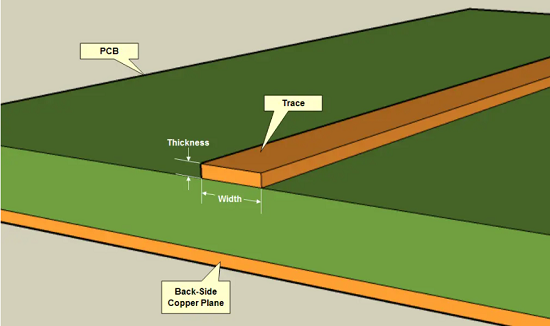
Step 2: Determine trace impedance, R (Ω).
This should be set and can be controlled during board fabrication
Step 3: Determine the maximum current flow for the trace, I (A).
Current can be determined from either of the following equations:
I = V2/R or I = P/V or I = √(P/R)
Step 4: Determine the expected temperature rise, T (°C).
This should be known or can be estimated from circuit operation design.
Step 5: Determine the trace cross-sectional area, A (mils2).
Use curve fitting constants, k, b and c, to approximate the IPC-2152 curve that relates area to current carrying capacity.
--For internal layers: k = 0.024, b = 0.44, c = 0.725
--For external layers: k = 0.048, b = 0.44, c = 0.725
A = (I/(k×Tb))1/c
Step 6: Determine the trace width, w (mils).
This should be set.
Step 7: Determine the PCB copper thickness, ? (mils).
? = A/w
PCB design software might allow you to set the copper thickness or it may require that you utilize copper weight values, which is also common among contract manufacturers. These parameters are directly proportional and you can convert to copper weight using the following equation:
Copper weight(oz) = (copper thickness(mils)) / 1.37
Essentially, one square foot of copper has a weight of 1 ounce.
Ensuring your PCB is designed with the right copper weight and copper trace width is crucial in ensuring your board works right the first time. Reengineering and extra prototyping fees are never things you want to have to explain to upper management or investors so it is important to understand the role that copper trace width and weight have in PCBA and electronics.
In PCBs, traces are conductors made of copper that have width, length, weight and thickness specifications. Current flow is reliant upon the choice of these parameters. In situations where trace length and width cannot be changed due to board density and spacing requirements, the variable to change to maximize current flow would be PCB copper thickness and or weight. Something to always pay attention to during the design process is signal integrity. Signal integrity in its simple form measures the quality of the electrical signal. For circuit boards, current loss and signal integrity depends on the amount of impedance encountered along its copper traces.
Heavy Copper PCBs are most commonly utilized in power electronics devices, or other products that may be subjected to harsh environments. These thicker traces result in greater durability while also allowing the traces to carry a larger amount of current without trace length or width being increased. On the other end of the spectrum, lighter copper weights are sometimes utilized in order to achieve a specific trace impedance without requiring an extremely small trace length or width.
Utilizing PCB copper thickness to optimize current flow, requires understanding how the two are intertwined. To start, let’s dive into how copper trace fabrication occurs and its implications in signal integrity.
1.PCB Copper Thickness in the Fabrication Process
One of the fabrication steps in creating bare boards is etching. Both the surface and internal layers are done with this process. This starts with a laminate sheet that is completely covered by copper. During the etching process, excess copper is removed from traces and other areas on the circuit board, such as on pads for parts and annular rings for vias. This is done using an ammonia-based solution.
Most shops/their suppliers have standardized starting copper sheet thickness. For example, for 1oz (0.0014in or 0.035mm) copper thickness, the sheet would have a 0.5oz (0.0007in or 0.018mm) layer of copper on both sides. What they can do with this thickness is etch it down to decrease or even plate it up to increase thickness in order to meet the desired specification. These sheets have some roughness to them due to their manufacturing processes. This can help with bonding to the dielectric material but at the same time it can also have an increasingly adverse effect on signal integrity at higher frequencies. With frequencies above 100MHz, the skin effect, in which current flow is typically close to the internal surface of a trace as opposed to through the conductive center, occurs, causing the effective resistance of the trace to increase and oppose current flow.
With plated vias, traces must be added after the holes in the board are drilled. One of the processes for accomplishing this is electrodeposition. In this process the board is placed in an electrolytic solution which contains copper ions. Next, a direct current is applied to set up a potential across the via and ions are distributed throughout the via. This distribution of the copper ions throughout the via or the filling determine the quality of signal flow along via traces. Understanding the fabrication process in PCB and PCBAs will help you in the design process.
2.Signal Flow and PCB Copper Thickness
PCB fabrication shops purchase sheets of copper at set thickness and weight from their suppliers. From their perspective, these are fixed numbers. From an engineer’s point of view, these parameters can be changed after fixing trace lengths and widths in order to optimize signal flows or the inverse to improve signal integrity. IPC-2152, the Standard for Determining Current-carrying Capacity in Printed Board Design, introduces trace parameters which includes copper weight, copper thickness, as well as trace width and trace length. These variables work together and depend on the properties of electrical/thermal material. There is much nuance to how all of these work together but there are a few simplified equations and calculators that can be used throughout the design process that will be adequate in 99% of cases.
PCB Blog
Contact Us
E-mail: [email protected]
E-mail: [email protected]
Skype: [email protected]
Whatsapp: +86 15012972502
Add: 2F, BUILDING H, WANDA INDUSTRIAL ZONE, ZHOUSHI ROAD, LANGXIN COMMUNITY,SHIYAN STREET, BAO 'AN DISTRICT, SHENZHEN, GUANGDONG, CHINA


 Skype Chat
 WhatsApp
  Mail inquiry