

How Do I Know If My PCB Solder Mask File Is Correct?
How Do I Know If My PCB Solder Mask File Is Correct?
The best way to review where mask will be applied is to look at your top copper layer and your top mask layer at the same time. They should be aligned so you can see exactly where mask clearances will be in relation to the copper. Anywhere you see a mask pad on the mask layer is where mask will NOT be applied. Do the same review for your bottom layer.
By default, we assume the entire board will be covered with solder mask, on both top and bottom sides of the board. If you don't want solder mask on your board, please make a note of this in your fabrication drawing, readme.txt or in the notes of your online order.
Your Gerber output should contain a separate mask file for the top and bottom layers. If you have a 100% through hole design, and the solder mask clearances are identical for the top and bottom sides, we can use the same file for both but please note this in your fab notes or on your order so we know this is what you intend for us to do.
1.What Size Should My Mask Clearances Be?
We see design files created by all types of software packages and engineers of varying degrees of experience. Sometimes the solder mask clearances are exactly the same size as the copper pad they are exposing, sometimes they are much larger or smaller.
We recommend a 2mil (0.05mm) swell on all sides. If your design rules are set much larger or smaller than this, we will automatically adjust the swell to be around 2mil.
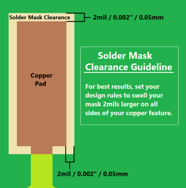
As a general rule, we will resize mask clearances to be approximately 2mils larger on each side of the copper feature to ensure it isn't partially covered with mask. As with everything else, there is a tolerance on the exact placement of the mask on a PCB. The tolerance for mask placement is ± 2mils (±0.05mm) of its intended true position. Even if mask alignment is shifted by the full 2mil tolerance, your entire copper pad should be still solderable.
TIP: If you are intentionally making your mask clearance smaller than the copper feature it's exposing; this is called a Solder Mask Defined pad (SMD). This is ok to do but please let us know this is your intent, otherwise the order may go on engineering hold or it may be automatically resized per our standard tooling process to be larger than the copper feature.
2.Solder Mask Defined Pads (SMD)
A Non-Solder Mask Defined (NSMD) pad is a traditional solder mask clearance that's larger than the copper pad it's exposing. Most solder mask apertures are NSMD. The mask clearance will be approximately 1.5mil-2mils (0.038mm - 0.05mm) larger than the copper feature on all sides to ensure no mask is accidentally printed on the copper. This is to prevent mask from accidentally being applied over the copper surface, thereby reducing the solderable surface area making soldering more difficult.
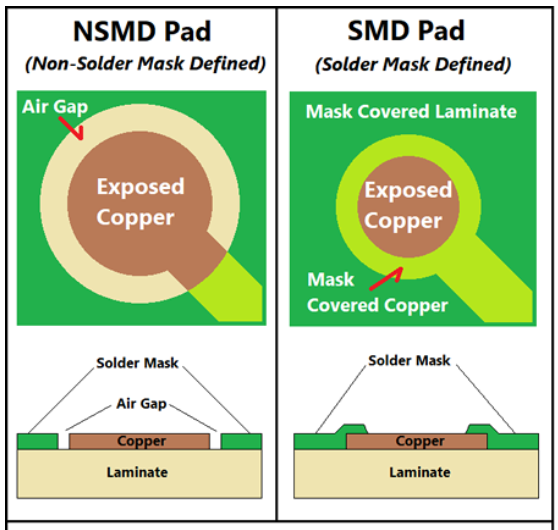
A Solder Mask Defined (SMD) pad has a solder mask clearance that is smaller than the copper feature and mask is intentionally printed over a portion of the copper. This is typically only seen on very tightly spaced footprints like BGAs where there simply isn't enough room to print a NSMD with the appropriate clearances.
When designing a solder mask defined pad, make your copper pads as large as you can so a complete copper pad will be exposed in the mask. There is a tolerance on the actual mask placement, so if the mask is only slightly smaller than the pad, there's a chance the mask could shift enough exposing bare laminate which would result in even less solderable surface area. A good rule of thumb is to have a large enough copper pad that will allow you to print at least 3mils (0.076mm) of mask on all sides of your copper pad.
3.Should I Put Solder Mask Between All Surface Mount Pads?
The short answer is yes, put them between as many pads as you can and cover as much of the board as you can. Mask dams will increase the likelihood the solder will remain in the desired location and you'll have a stronger solder joint. When solder reflows, it liquefies and can easily run, resulting in solder starvation. Symptoms of solder starvation are:
--Intermittent Connection
--Intermittent Shorts
--Poor Solder Joint Strength
--Increased Inspection Time
--Increased Rework
--Higher RMA Costs for Field Failures

Traditional "dog-bone" pattern BGAs (ball grid arrays) are especially prone to solder starvation due to the proximity of open vias close to the footprint of the chip. We always recommend filling those vias that are underneath or very close to BGAs, with a non-conductive epoxy and applying solder mask over the top of the hole to prevent solder run off.
Other techniques used to handle this issue are the use of Via In Pad (a.k.a. Active Pad) and Solder Mask Defined Pads, confusingly sometimes abbreviated SMD.
More information on Via In Pad can be found in our article on what's the difference between the different via types?
Click here to know:What is Solder mask and why do you need solder mask?
PCB Blog
Contact Us
E-mail: [email protected]
E-mail: [email protected]
Skype: [email protected]
Whatsapp: +86 15012972502
Add: 2F, BUILDING H, WANDA INDUSTRIAL ZONE, ZHOUSHI ROAD, LANGXIN COMMUNITY,SHIYAN STREET, BAO 'AN DISTRICT, SHENZHEN, GUANGDONG, CHINA


 Skype Chat
 WhatsApp
  Mail inquiry