

Design tips about Blind & Buried vias
Design tips about Blind & Buried vias
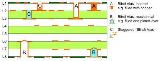
Due to the increasing complexity of design structures blind vias and buried vias are increasingly used in high-density circuit boards (HDI-PCB).
*A blind Via connects exactly one outer layer with one or more inner layers.
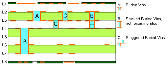
*A buried via is a via between at least two inner layers, which is not visible from the outer layers. This technology allows more functionality in less board space (packing density).
Suggestion:For cost reasons, we recommend avoiding an overlap of blind and buried vias in the layer build-up! For example, avoid blind vias from L1 - L3 and simultaneously buried vias from L2 - L4.
--Blind Via
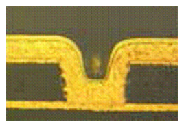
Blind vias are used to connect one outer layer with at least one inner layer.The holes for each connection level must be defined as a separate drill file.The ratio of drill diameter to hole depth (aspect ratio) must be 1:1 or larger. The smallest hole determines the depth and thus the max. distance between the outer layer and the corresponding inner layers.
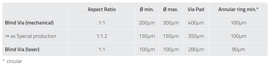
Design Parameters for Blind Via
Optional: Via-in-Pad
You can also place your blind vias within pads.
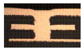
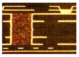
--Buried Via
Buried vias are used to create connections of the inner layers, which have no contact with the outer layers.
The holes for each connection level must be defined as a separate drill file.
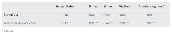
The ratio of drill diameter to hole depth (aspect ratio) must be 1:12 or larger.
The smallest hole determines the depth and thus the max. distance between the respective inner layers.
Suggestion:Generally: The larger you choose the annular rings on the inner layers, the more stable the connection.
Design Parameters for Buried Via
Optional: Filled Buried Via
Buried vias with a min. Ø of 150µm (0.150mm) can be filled galvanically.
Additional information:
--PCB Drills & Throughplating
PCB Blog
Contact Us
E-mail: [email protected]
E-mail: [email protected]
Skype: [email protected]
Whatsapp: +86 15012972502
Add: 2F, BUILDING H, WANDA INDUSTRIAL ZONE, ZHOUSHI ROAD, LANGXIN COMMUNITY,SHIYAN STREET, BAO 'AN DISTRICT, SHENZHEN, GUANGDONG, CHINA


 Skype Chat
 WhatsApp
  Mail inquiry