

Products >> PCB manufacturing >> RF PCB
Rogers high frequency PCB Ro4350B RF circuit boards
- Product No.:202045232417
- PCB board thickness:0.13-8.0mm(Double side),0.4-8.0mm(Multi-layer)
- Layer count:4-32 layer
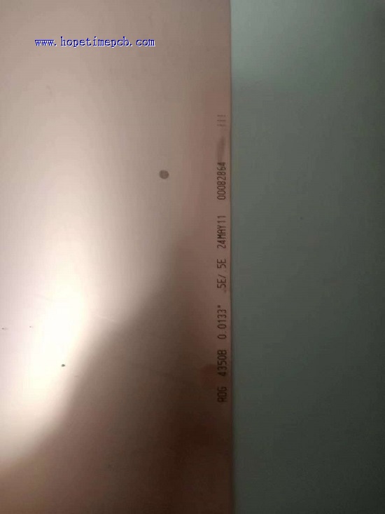
- PCB material:RO4350B 20MIL
- Copper thickness:0.5OZ,1OZ
- Surface treatment:ENIG 2U
- Soldermask:Green
- silkscreen:White
- D.K:3.48
- D.F:0.0037
Rogers high frequency PCB Ro4350B RF circuit boards
Rogers high frequency PCB application
PCB with RF (radio frequency) are an increasingly used technique within the Printed circuit board industry.
--A high frequency printed circuit board with works above 100 MHz.
--Works above 2 GHz radio frequency is a Microwave circuit board.
RF PCBs are used in different applications such as remote controls(wireless controls) smart phones,sensors, security,Amplifer,Radar etc.
New technologies make more and more use of these RF applications.This asks for a manufacturing according to high quality standards and
choosing the right RF materials depending on the application.
Specific for Rogers high frequency pcb
*High-frequency PCBs are mainly used in radio and high-speed digital applications, such as 5G wireless communications, automotive radar sensors, aerospace, satellites, etc. But there are many important factors to be considered when manufacturing high-frequency PCBs.
*The material we used are Rogers RO4350B / RO3003 / RO4003 / RO3006 / RT/Duroid 5880 / RT5870 and etc.PTFE F4BM /Arlon / Isola / Taconic /Teflon material ect.
*Dielectric constant ranging from 2.2 to 10.6
*The main products are PTFE high frequency PCB board,3G/4G/5G smart antenna PCB,Power amplifier printed circuit board,Low noise amplifier electronic board,Divider circuit boards,duplexer PCB,Filter circuit board.coupler PCB and other radio frequency (RF) communication products.
*The main RF PCB types are Rogers / PTFE high frequency / copper clad / microwave / polytetrachloroethylene / Teflon / Taikangike / Yalong
What is the ideal RF( Radio frequency )PCB stack up?
It depends on your working frequency and target impedance. but in general rule you should avoid pushing the limits of pcb factory tolerances. for instance if you are using 50 ohm microstrips and your track width is 0.15 mm. this is not ideal because of manufacturing tolerances. at the end result this line could be a 0.12 or 0.18 mm. this is almost %20 change in width. so i always try to choose larger size than 0.5 mm tracks for micropstrips. also you should be careful about prepreg materials and resin content. other possible solution is manufacturing your pcb with impedance controlled.
When it comes to the ideal RF PCB stackup, various methods are used to PCB RF design that are microstrip, suspended strip, coplanar waveguide and grounding. You know, a microstrip consists of a fixed length of metal or wire and the under entire or part of the ground plane. Furthermore, the characteristic impedance of microstrip structure is basically from 50Ω to 75Ω.
There are some sample Stack up for your reference.
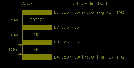
1.4L board stack up for RO3003 + FR4 Mixed laminate RF PCB
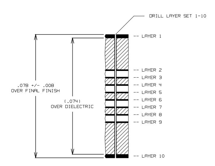
2.10 Layer of stack up for mixed dielectric of RO4350B + FR4 RF PCB.
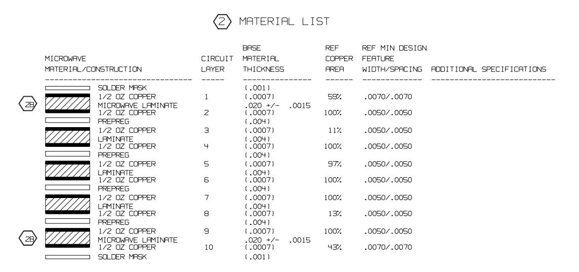
3.10 Layer of stack up for mixed dielectric of RO4350B + FR4 RF PCB.
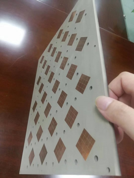
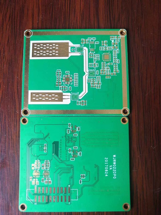
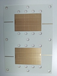
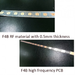
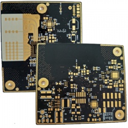
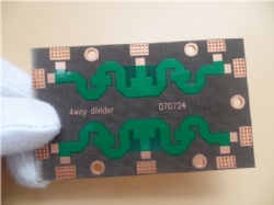
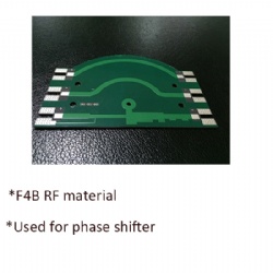
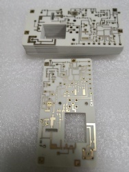
Some of our RF PCB Project photo
*Please send inquiry to [email protected] directly!!!
Related Products
Products Category
- PCB Design & Layout
- PCB manufacturing
- PCB Assembly
- BGA Assembly
- THT Assembly
- SMT Assembly
- Mixed PCB Assembly in Electronic PCBA
- Single sided PCB assembly
- Double sided PCB assembly
- Rigid-Flex Assembly
- COB Bonding Manufacturing
- Components sourcing for PCB Assembly
- SMT Stencils
- Box build assembly
- PCB engineer reverse
Contact Us
E-mail: [email protected]
E-mail: [email protected]
Skype: [email protected]
Whatsapp: +86 15012972502
Add: 2F, BUILDING H, WANDA INDUSTRIAL ZONE, ZHOUSHI ROAD, LANGXIN COMMUNITY,SHIYAN STREET, BAO 'AN DISTRICT, SHENZHEN, GUANGDONG, CHINA


 Skype Chat
 WhatsApp
  Mail inquiry